
TEE314 Microelectronics Course Assignment 2 Brief 2026 | WOU
Assignment Type
Individual Assignment
Subject
TEE314 Microelectronics
Uploaded by Malaysia Assignment Help
Date
06/25/2026
TEE314 Course Assignment 2 – 25%
Submission Date: 19th July 2026 before 11:59:59pm.
Evidence of plagiarism or collusion will be taken seriously and the University regulations will be applied fully. You are advised to be familiar with the University’s definitions of plagiarism and collusion.
Instructions
- This is an individual assignment. No duplication of work will be tolerated. Any plagiarism or collusion may result in disciplinary action, in addition to ZERO mark being awarded to all involved.
- You are to submit online of your answers in OAS system and it is your responsibility to submit your Assignment correctly and timely. OAS system doesn’t allow re-submission of assignment. Marks will be awarded for correct working steps and answer.
- The total marks for Assignment 2 is 100 and contributes 25% towards the total grade.
- Assignment 2 covers all topics from your course material.
- Assignment 2 consist of online lab sessions.
- You are expected to write a lab report upon the completion of your lab exercises and submit it to OAS. Your tutor will be able to guide you on the outlines of the report. A rubric will be used to assess your lab work. Please look at the last page of your lab sheet for the rubric.
- Your assignment must be word processed (single spacing) and clearly laid out. Any additional appendices or attachments must be placed at the end of the submitted document and must be referred to in the main body of the assignment, or it will not be read by the marker. Marks will be deducted from handwritten and/or photo snap shot assignments.
- All files or documents submitted must be labelled with your WOU ID and name.
- Answer all parts in English. All necessary simulation results must be shown clearly.
- The use of Turnitin is not necessary for this assignment.
Introduction
Learner who has taken TEE314/05 Microelectronics course is mandatory to attend six hours practical session, which comprises of two practical each last for three hours. The practical session is to be carried out either in computer laboratory in the University or using own personal computer to be done at home.
The objectives of these practical sessions are meant for learner to use the knowledge from this subject and practice it by designing CMOS logic circuit and sequential circuit using schematic capture software and using these schematics convert them into layouts that suppose to be used for mask designs and eventually fabricated as integrated circuits.
This practical manual consists of four experiments and one assignment. The first experiment is a self exploratory experiment consists of two parts aimed with the objectives for the learner to learn how to use schematic capture software named “Dsch3.exe” and to learn how to use Microwind layout software named “Microwind3.exe”.
First part of the experiment, learner learns how to use the commands and library templates of schematic capture software to design both logic gate circuits and sequential circuits using both p-channel and n-channel MOSFETs, logic gates or combination of them. Besides learning the designs, learner also learns simulation, checking results of simulation. The conversion of complex logic gate circuits and sequential circuits into high level schema symbol and other features/capability of the software like generate of verilog list and generation of SPICE list are to be learned.
Second part of the experiment, learner learns how to us the commands and library templates of Microwind layout software to design/draw the layout of logic gates and sequential circuits. The learning including placing the various layers of the layout like the diffusion level, polysilicon gate layer, metal layer, interconnect via, and biasing of substrate. Upon completion of layout, design rule check and simulation are always to be done to check if there is violation of the rule and if the layout is performing to expectation. Other features of the software to be learned are viewing the 3-D structure of the layout, compilation of layout from a verilog file and from a logic statement.
Experiment 2 is aimed to design n-MOSFET and p-MOSFET according to specifications and to design simple 2 input exclusive OR gate circuit.
Experiment 3 is aimed to design a 4-bit full adder circuit and a 1-bit comparator and simulate the results. The designs include designing the circuit using basic n-channel and p-channel MOSFETs and the layout of the circuits.
Experiment 4 is aimed to design a bi-state memory element circuit, a simple D-flip flop and a T-flip flop. Like experiment 3, the learner has to design the schematic circuits using basic n-channel and p-channel MOSFETs, draw the layouts of these circuits, and simulate the circuits to observe the expected results of the designs.
Practical assignment is aimed to design a VLSI integrated circuit chip that performs the function as stated in the definition of system. This is a non-standard design. Learner has to utilize the knowledge of state machine combining with the knowledge learnt from this subject to design and simulate the result as according to design definition.
Experiment 1 – Familiarization of Using Microwind VLSI Layout Software and Schematics Capture software
1.0 Objectives
- To learn how to use schematic capture software DSch3.
- To learn how to use Microwind layout software Microwind3.
1.1. Material Requirements
- Microwind and Dsch software, computer, and reference book.
1.2 Introduction to Software
The MICROWIND version 3 program allows the learner to design and simulate an integrated circuit at physical description level. The package contains a library of common logic and analog ICs to view and simulate. MICROWIND3 includes all the commands for a mask editor as well as a 2D and 3D process view and Verilog compiler. The example of the layout is shown in Fig. 1.1.
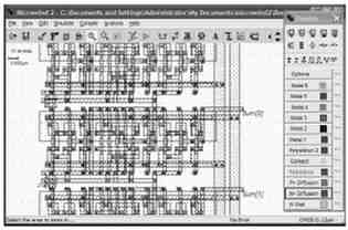
Figure 1.1: The layout of an integrated circuit
The right hand side of the screen showing the palettes that consists of various layers drawing palette right from p-diffusion, n-diffusion, n-well, polysilicon 1, polysilicon 2, contact via, various metal layers, power supply, input stimulant, output display etc.
The DSCH version 3 program is a logic/transistor level capture software and simulator. DSCH3 is used to validate the architecture of the logic circuit before the microelectronics design is started. An example of the design is shown in Fig. 1.2.
The symbol library consists of various logic gate components, basic n-channel and p-channel MOSFETs, power supply, display, and advanced components such as voltage source, switches etc.
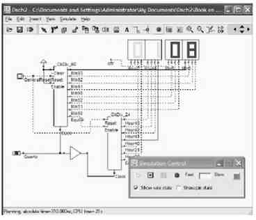
Figure 1.2: The design using DSCH schematic capture software
1.3 Familiarization with the Layout Drawing Schematic Capture and Layout Softwares
There are countless of VLSI layout softwares available in the market. The price to obtain these softwares ranges from free to charge to millions of dollar. Learner can browse this website http://www.vlsitechnology.org/html/ic_software.html to obtain more the information. For learning purpose, let’s choose Microwind software. Light version of Microwind software, which is free of charge, can be obtained from this website http://www.microwind.org. This software package comes with two parts, which are the schematic capture software and layout software. The schematic software – “Dsch.exe” allows learner to design logic circuit, which can be combinational and sequential types using basic logic gates or p-channel and n-channel MOSFETs. The layout software “Microwind.exe” allows learner to design layout manually or draw layout automatically by importing a verilog file.
1.4.1 Schematic Capture
The manual page of the schematic capture software “Dsch.exe” is shown in Fig. 1.3. The manual contains functions, open file, save file, select, cut, copy, move, rotate, add line, simulate, timing diagram, zoom in, zoom out, view electrical list, move, symbol libraries, and working area. The symbol libraries consist of basic gate and input pad and output display. The symbol libraries also consist of some advanced electrical components and sources. At the right bottom of the display shows the default technology used. In this screen it shows the default technology is 0.12µm.
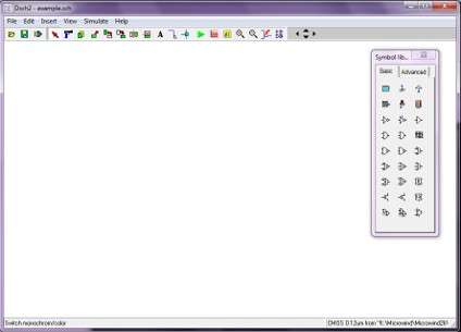
Figure 1.3: The manual page of schematic capture software
Learner may begin to design logic gate using p-channel MOSFET and n-channel MOSFET. If we are to design a CMOS inverter as shown in Fig. 1.4, which has logic function output = , the logic function can be interpreted as low asserted high and high asserted low equation. This shall mean a p-channel and an n-channel MOSFET are connected in series with input A and output taken from the drains of the transistors. The source of p-channel MOSFET is connected to VDD power line, whilst the source of n-channel MOSFET is connected to VSS ground line. To get the transistor, it is done by pressing the transistor and placing it into the working area. To interconnect, it is done by using ‘add line’ function. The power VDD and ground VSS can be connected in the similar manner i.e. pressing them from the symbol libraries and placing them at the right place in the working area. Upon finishing doing the above stated steps, learner has to connect the input pad and output display, which are shown as a square pad and ‘LED’ like bulb from the symbol libraries. To ensure that the connection is done properly, learner has to make sure that there is connecting node at the connection.
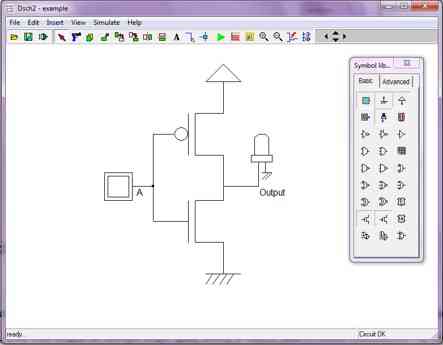
Figure 1.4: The design of an inverter
Upon design, you can press the ‘simulate’ key to simulate the functionality of the inverter. The display is shown in Fig. 1.5. The colour display showing logic 1, while white colour display showing logic 0, learner may toggle the input by placing the cursor on the input pad and press the left hand button of the mouse for toggling as shown in Fig. 1.6 after toggling. Both schematics also display the switching stage of the MOSFETs.
The result of the simulation can be viewed by pressing the ‘timing diagram’ key, which is shown in Fig. 1.7. From the timing diagram, it shows that the inverter is function correctly. This is because when input is at logic 0, output is at logic 1 and vice versa.
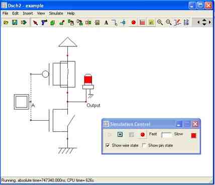
Figure 1.5: Simulation screen for an inverter
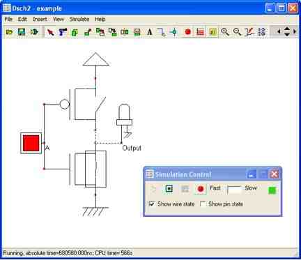
Figure 1.6: Simulation screen for an inverter
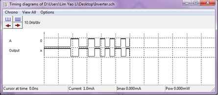
Figure 1.7: Timing diagram of an inverter
The logic function of a three input NAND is output = . This equation is a high asserted low equation, which can be used to design n-channel MOSET network of the NAND gate. For designing the CMOS version of this NAND gate, we need also a p-MOS network circuit, which is a low asserted high network. This can be done by using DeMorgan theorem to convert logic function output = to output = , which is a low asserted high equation. The transistor level of a three input NAND gate is shown in Fig. 1.8. It is done by dragging the n-channel MOSFET and p-channel MOSFET transistors to the working area and inter-connect them and putting the VDD power line and VSS ground line.
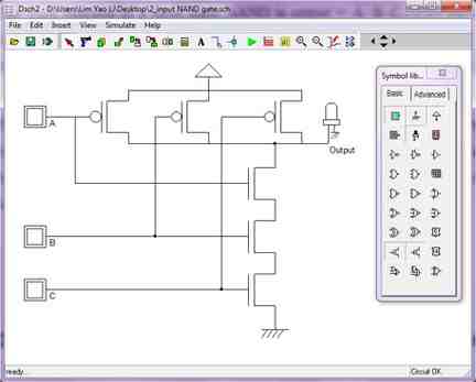
Figure 1.8: The design of a 3-input NAND gate
The result of simulation is shown from the timing diagram in Fig. 1.9. From the timing diagram, it shows that the 3-input NAND gate is functionally working.
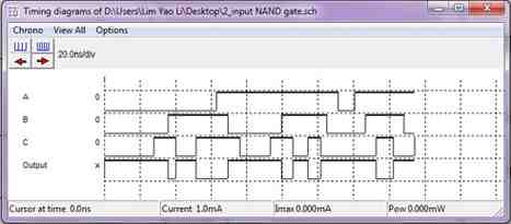
Figure 1.9: Timing diagram of the 3-input NAND gate
Supposing that you have a complex schematic circuit that you would like to it to be represented by a ‘black box’ block, you may ‘Schema to new symbol’ function to achieve it. Let’s look at an example shown in Fig. 1.10. This circuit has two inputs and two outputs. BY pressing ‘Schema to new symbol’ function, a schema block is created as shown in Fig. 1.11. The block can then be used in the subsequent design.
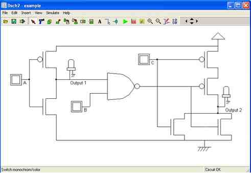
Figure 1.10: A complex logic circuit
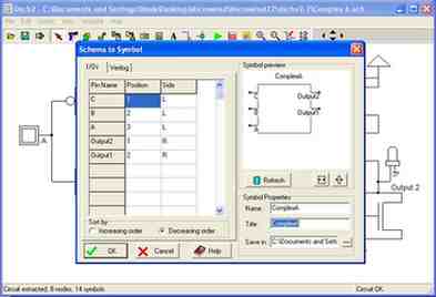
Figure 1.11: A schema block for the complex circuit shown in Fig. 1.10
A verilog list can be created for any schematic circuit that can be used as the input file for creating layout. Once ‘Make Verilog file’ function is pressed, the verilog list is created as shown in Fig. 1.22.
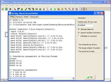
Figure 1.12: Verilog list of the complex logic circuit shown in Fig. 1.10
A SPICE file can be created by pressing ‘Create SPICE File’ function that showing SPICE list in Fig. 1.13. The created SPICE list can be used for simulation with SPICE simulator.
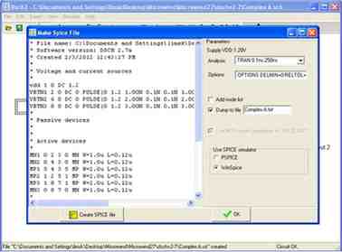
Figure 1.13: SPICE list of the complex logic circuit shown in Fig. 1.10
1.4.2 Layout
The manual page of the layout “Microwind.exe” is shown in Fig. 1.14. The manual contains the functions, open file, save file, select, cut, copy, move and stretch, simulate, timing diagram, zoom in, zoom out, view electrical node, 2D view, 3D view, ruler, design rule check, palette function, and the working area. The palette consists of basic n+ and p+ diffusion layers, polysilicon 1 and 2 layers, metal 1 to metal 6 layers, power sources, via connections, passive and active components, and MOSET generator. At the right bottom of the display shows the default technology used. In this screen it shows the default technology is 0.12µm.
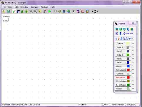
Figure 1.14: The manual page of Microwind layout software
Vertical layout approach is recommended i.e. placing the poly gate line vertically and power line horizontally. This approach will be adopted for the rest of design mentioned in this text.
Let’s proceed to design the layout of an inverter as shown in Fig. 1.4. One of approaches is to use the ‘MOS generator’ function in the palette. Upon selecting ‘MOS generator’ function, you can choose either n-channel MOSET, p-channel MOSET, or double gate transistor. Since the inverter has one input, you will choose one finger type. Beside these options, you may choose low leakage, high speed or high voltage type. The layout is shown in Fig. 1.15. From the colour illustration you will see that the p-channel MOSET is sitting inside an n-well. The ‘cross square’ pad is the via that connecting the semiconductor either the p-diffusion or n-diffusion type to the first metal 1, which is in blue colour. The orange colour bar is the polysilicon gate. The grid is used for ease for drawing layout and there is a scale of 5 lamda, which equivalent to 0.30µm. You may choose ‘zoom in’ or ‘zoom in’ function to change the scale. Since the substrate material for CMOS VLSI design is a <100> p-type semiconductor, thus, the black work area is a p-type substrate.
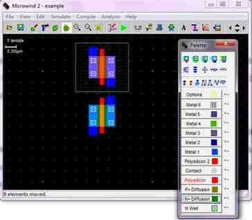
Figure 1.15: Layout of a p-channel and an n-channel MOSFET
Upon designing or placing the transistors, the next step is to interconnect them according to the design and placing the power line horizontally, bias the p-substrate and n-well, connect input source, and connect visible node. Figure 1.16 shows the layout after these layout steps. The layout shows that the source of the p-channel MOSET is connected to power line VDD via metal 1, whilst the source of n-channel MOSET is connected to VSS ground via metal 1. The drains of both the transistors are connected together to form the output. The p-substrate is biased with VSS, whilst the n-well is biased with VDD source. You may want recall the reason the p-substrate and n-well needed to be biased in this manner.
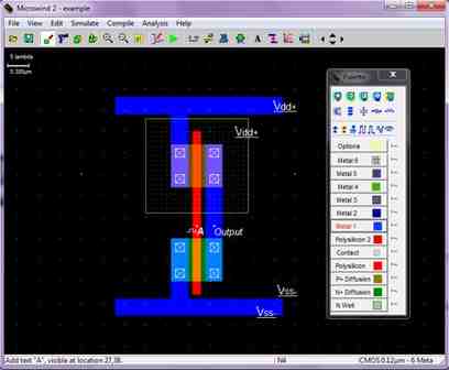
Figure 1.16: Layout of an inverter
Upon design the layout of the inverter, you may want simulate to see if it is functioning. This can be done by selecting simulation function. The result of the simulation is shown in Fig. 1.17, which is right as expected for an inverter.
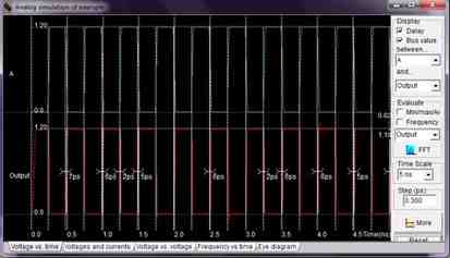
Figure 1.17: Simulation result of the layout of an inverter
Let’s discuss how to design the layout of three series connected transistor as shown in Fig. 1.18. You may begin with the ‘MOS generator’ function and follow by choosing n-channel MOSET with three fingers. You shall then remove extra via contacts and metal 1 using ‘cut’ function. Figure 1.19 shows the layout after connected the source of transistor C to VSS ground, bias the p-substrate with VSS ground, and placing the input source to input A, B, and C.
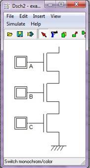
Figure 1.18: The transistor circuit of three series n-channel MOSETs
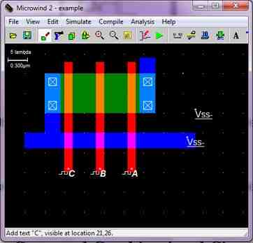
Figure 1.19: The layout of three series n-channel MOSETs
Let’s discuss how to design the layout of three parallel connected transistors as shown in Fig. 1.20. You may begin with the ‘MOS generator’ function and follow by choosing p-channel MOSET with three fingers. Figure 1.21 shows the layout after connecting the VDD power line, bias the n-well with VDD voltage, and connecting all sources and drains of the transistors together via metal 1.
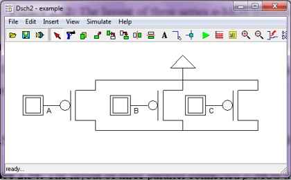
Figure 1.20: The transistor circuit of three parallel connected p-channel MOSETs
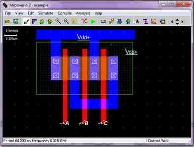
Figure 1.21: The layout of three parallel connected p-channel MOSETs
1.5 Drawing Layout of Logic Gates and Combinational Circuit
The following the same procedure, the layout of any logic gates and combinational circuit can be drawn. Taking for an example the transistor level circuit of the combinational logic with logic function output = is designed and shown in Fig. 1.16. Its layout is shown in Fig. 1.17. The simulation result is shown in Fig. 1.18.
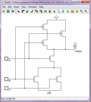
Figure 1.16: The transistor level design of combinational circuit output =
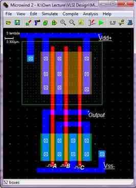
Figure 1.17: The layout of combinational circuit output =
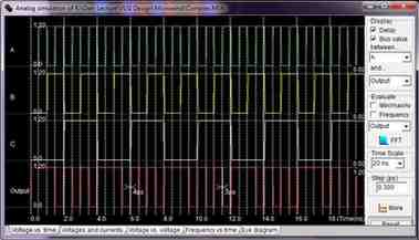
Figure 1.18: The timing diagram of combinational circuit output =
Experiment 2 – Design of Simple Transistors and Logic Circuit
2.0 Objectives
- To design n-MOSFET and p-MOSFET according to specifications.
- To design simple logic circuit.
2.1 Material Requirements
Microwind and Dsch software, computer and your course material.
2.2 Procedure
- Design an n-MOSFET that has aspect ratio of 5 and drain and source width of 8l using a 0.12 mm technology.
- Simulate its output characteristic using Model 1 SPICE.
- Display the output characteristic.
- Design a p-MOSFET that has the output current characteristics of the n-MOSTFET designed earlier using a 0.12 mm technology.
- Simulate its output characteristic using Model 1 SPICE.
- Display the output characteristic
- Comment the difference in terms of the designed aspect ratio.
- Draw the transistor level logic function f(A,B) = using Dsch software
- Prove the functionality of the function f(A,B) = by shown the logic diagram.
- Draw the layout of the logic function f(A,B) = using Microwind
- Show timing diagram of the functionality of the logic function f(A,B) =
- Conclusion of the experiments
Experiment 3 – Design of Complex Logic Circuits
3.0. Objectives
- To design a 1-bit full adder circuit
3.1. Material Requirements
- Microwind and Dsch software, computer, and course material.
- 12mm technology is to be used for all designs.
- Design rule should be observed closely.
- Minimum dimension for all designs is required.
3.2. Procedure
- Design a 1-bit full adder using Dsch software.
- Display the schematic of the design.
- Show the simulated results pertaining to the functionality of the adder
- Use Microwind software to draw the layout of the designed 1-bit full adder.
- Display the layout of the design.
- Display the simulated result pertaining to the functionality of the design.
- Conclusion of the experiments
Experiment 4 – Design of Sequential Logic Circuits
4.0 Objectives
- To design a bi-state memory element circuit.
- To design a T-flip flop.
4.1 Material Requirements
- Microwind and Dsch software, computer, and reference book.
- 12 mm technology is to be used for all designs.
- Design rule should be observed closely.
- Minimum dimension for all designs is required.
4.2 Procedure
- Design a bi-state memory element circuit using Microwind software.
- Display the layout of the design.
- Show the simulated results pertaining to the functionality.
- Design a T-flip flop using DSch software. (No Need Simulation)
- Display the design.
- Make a Verilog file of the design.
- Compile the Verilog file using Microwind software.
- Display the layout of the design.
- Check the functionality of the design by displaying the functional results.
- Conclusion of the experiments
Rubric For TEE314 Assessing Lab Reports
| 1
Beginning or incomplete |
2
Developing |
3
Accomplished |
4
Exemplary |
Score |
|
| Introduction
(5%) |
Very little background information provided or information is incorrect | Some introductory information, but still missing some major points | Introduction is nearly complete, missing some minor points | Introduction complete and well-written; provides all necessary background principles for the experiment | |
| Experimental procedure
(10%) |
Missing several important experimental details or not written in paragraph format | Written in paragraph format, still missing some important experimental details | Written in paragraph format, important experimental details are covered, some minor details missing | Well-written in paragraph format, all experimental details are covered | |
| Results:
data, figures, graphs, tables, etc. (25%) |
Figures, graphs, tables contain errors or are poorly constructed, have missing titles, captions or numbers, units missing or incorrect, etc. | Most figures, graphs, tables OK, some still missing some important or required features | All figures, graphs, tables are correctly drawn, but some have minor problems or could still be improved | All figures, graphs, tables are correctly drawn, are numbered and contain titles/captions. | |
| Discussion
(30%) |
Very incomplete or incorrect interpretation of trends and comparison of data indicating a lack of understanding of results | Some of the results have been correctly interpreted and discussed; partial but incomplete understanding of results is still evident | Almost all of the results have been correctly interpreted and discussed, only minor improvements are needed | All important trends and data comparisons have been interpreted correctly and discussed, good understanding of results is conveyed | |
| Conclusions
(10%) |
Conclusions missing or missing the important points | Conclusions regarding major points are drawn, but many are misstated, indicating a lack of understanding | All important conclusions have been drawn, could be better stated | All important conclusions have been clearly made, student shows good understanding | |
| Spelling, grammar, sentence structure
(15%) |
Frequent grammar and/or spelling errors, writing style is rough and immature | Occasional grammar/spelling errors, generally readable with some rough spots in writing style | Less than 3 grammar/spelling errors, mature, readable style | All grammar/spelling correct and very well-written | |
| Appearance and formatting
(5%) |
Sections out of order, too much handwritten copy, sloppy formatting | Sections in order, contains the minimum allowable amount of handwritten copy, formatting is rough but readable | All sections in order, formatting generally good but could still be improved | All sections in order, well-formatted, very readable |
Get Expert Help With TEE314 Course Assignment 2
Get Help By Expert
Are you also finding it difficult to complete your TEE314 microelectronics course assignment 2? Many WOU students struggle with CMOS logic circuit design, Microwind and DSCH simulations, Verilog generation, VLSI layouts, and writing a well-structured lab report that meets the marking rubric. Malaysia Assignment Help has supported students with similar engineering assignments through expert-written solutions. You can also explore our engineering assignment help, and WOU assignment questions. If you need a professionally written lab report that follows your university requirements, our report writing help is here to support you.

Recommended Assignments for You
Related University Assignments
- TEE314 Microelectronics Course Assignment 2 Brief 2026 | WOU
- MPU3193 /MCMPU3193 Philosophy and Current Issues Assignment 2, 2026
- MCBMG311/03 Micro – Credential in Employment Law and Industrial Relations Assessment 3 Question 2026 | WOU
- TEE208/03 Circuit Theory II Assignment 2, 2026 | Wawasan Open University
- TEL 203/03 Process Control and Instrumentation Course Assessment 2 (CA2 – 30%)
- The Challenges Teaching English to Refugee Children Research Proposal Case Study
- TEE106/03 Basic Electromagnetic Theory Assignment 1 (25%)
- WUC118/03 Computing & Digital Transformation Assignment: Case-Based Analysis on Cloud, Cybersecurity & Emerging Technologies
- BMG 323/03 (BBM023/03) Clustering and Predictive Analysis Assignment 2: Homestay Case Study for Data-Driven Business Optimization in Malaysia
- BBM205 MCBBM205 Course Assignment(25%) January 2025 WAWASAN Open University : Basic Accounting

Convincing Features